


About IDER
The IDER unit is a new education and research platform, generally consisting of young researchers, including academic staff, postdoctoral researchers and doctoral students, from two or more laboratories of COE program members. Some IDER units are established specifically for collaborations with other institutions, companies and overseas organizations.
COE program participating division
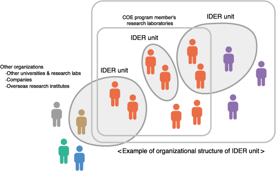
- Other organizations
- -Other universities & research labs
- -Companies
- -Overseas research institutes
- COE Program Member's Research Laboratories
- IDER unit
- IDER unit
- IDER unit
<Example of organizational structure of IDER unit>
We have built IDER units according to the following policies.
- Each unit must clearly define its strategic R&D goals.
- Complementary and cross-disciplinary collaboration units, which involve various research organizations in Japan and abroad with their developed own technologies, must be formed.
- The unit structure must be dynamically reinforced in response to the past development of research activities.
- The unit must provide a venue for young researchers to conduct independent activities.
IDER Units
| Research Project | Project Leader (Supervisor) |
|
|---|---|---|
| Flexible and printable organic optical devices | Dr. Hirotake Kajii (Prof. Yutaka Ohmori) |
|
| Advanced wide bandgap semiconductor | Prof. Masashi Yoshimura (Prof. Takashi Sugino) |
|
| Advanced bio-imaging system | Prof. Makoto Osanai (Prof. Tetsuya Yagi) |
|
| Concept invention for next generation power semiconductor devices |
Prof. Yushi Miura (Prof. Toshifumi Ise and Dr. Hideo Iwamoto) |
|
| Smart integrated sensing system | Prof. Toshimasa Matsuoka (Prof. Kenji Taniguchi and Prof. Mitsuhiro Katayama) |
|
| Simulation technology for electronic devices innovation | Prof. Nobuya Mori (Prof. Masaaki Kuzuhara) |
|
| Terahertz sensing and imaging systems | Dr. Iwao Kawayama (Prof. Masayoshi Tonouchi) |
|
| Advanced photonic devices for new-generation communication networks |
Prof. Masatoshi Fujimura (Prof. Toshiaki Suhara) |
|
| Plasma photonic device generating high luminescent electromagnetic radiation toward diagnostics of electronic device material |
Dr. Yuichi Inubushi (Prof. Ryosuke Kodama) |
|
| Exploration of new materials toward innovative electronic devices |
Dr. Norimasa Ozaki (Prof. Ryosuke Kodama) |
|
| High quality HTS-SQUID by improvement of GB junction properties |
Dr. Tetsuro Maki (Prof. Hideo Itozaki) |
|
| Advanced high-performance organic photovoltaic device | Prof. Akihiko Fujii (Prof. Masanori Ozaki) |
|
| Advanced optical electrical interface | Dr. Shintaro Hisatake (Prof. Tadao Nagatsuma and Prof. Yasuyuki Okamura) |
|
| Development of crystallization techniques of organic and macromolecular materials | Mr. Ryota Murai (Prof. Yusuke Mori) |