平成21年度 実績報告書
92/156
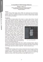
教育研究プラットフォームIDER研究成果/ポストドクター・GCOE研究員An Area - Efficient CMOS Bandgap Reference Bogoda A. Indika U. K. D ivision of Electrical, Electronic and Information Engineering , Graduate School of Engineering , Osaka University Taniguchi Laboratory Abstract An area efficient CMOS bandgap reference (BGR) with switched - current and curre nt - memory technique is presented. The proposed circuit uses only one parasitic bipolar transistor to generate reference voltage so that significant area reduction can be achieved. In addition, bipolar transistor device mismatch can be eliminated. Introdu ction A Key element of analog - to - digital (A/D) converters is a precise voltage reference with good stability against temperature and supply voltage. The most popular design to provide a precision voltage reference with low sensitivity to temperature and supply variation is the bandgap reference voltage generator (BGR). In conventional CMOS BGR the output voltage is derived from the voltage difference across two identical diodes forward biased by two unequal, precisely ratioed currents. In the conventional CMOS process, nearly ideal diode characteristics can be obtained from the base - emitter voltage V BE of parasitic substrate transistors. However, compared to other devices, parasitic transistors need larger area size. As CMOS technologies continues to sh rink, the design area becomes more expensive and thus an important aspect of any design. Despite the MOSFETs are scaled down to the nanoscale regime, parasitic bipolar transistors are left unchanged. Therefore the design area of the common conventional BGR , which uses area ratio of the parasitic bipolar transistors to generate reference voltage, becomes a critical problem. Another problem of the traditional BGR is no flexibility in output voltage. Because, as its name suggests, the output voltage is close t o the bandgap of silicon, which is approximately 1.2V at room temperature. To overcome this problem, references that output a fraction of the bandgap voltage have been demonstrated . However, such references require resistor networks with large values occ upying large design area. In This paper we present an improved BGR which is capable of generating reference voltage by using only one parasitic bipolar transistor, thus the area size becomes significantly smaller and bipolar transistors device mismatch is eliminated. Moreover the proposed circuit outputs a fraction of the silicon bandgap voltage, and the reference voltage V REF can be set to almost any value. Conclusion A novel area - efficient bandgap reference utilizing switched - current and current - memory techniques is presented. The proposed circuit is designed and simulated in 0 . 25 μm CMOS process. Th e simulation results show that the output reference voltage V REF is 650 mV, and the temperature coefficient of V REF is smaller than 10.4 ppm/°C for the temperature form 0 °C to 100 °C. The design area is less than 110 μm × 100 μm and consumes average suppl y current of 49.5 μA. Fig. 1 . Layout of Proposed BGR 88
元のページ